
Challenge
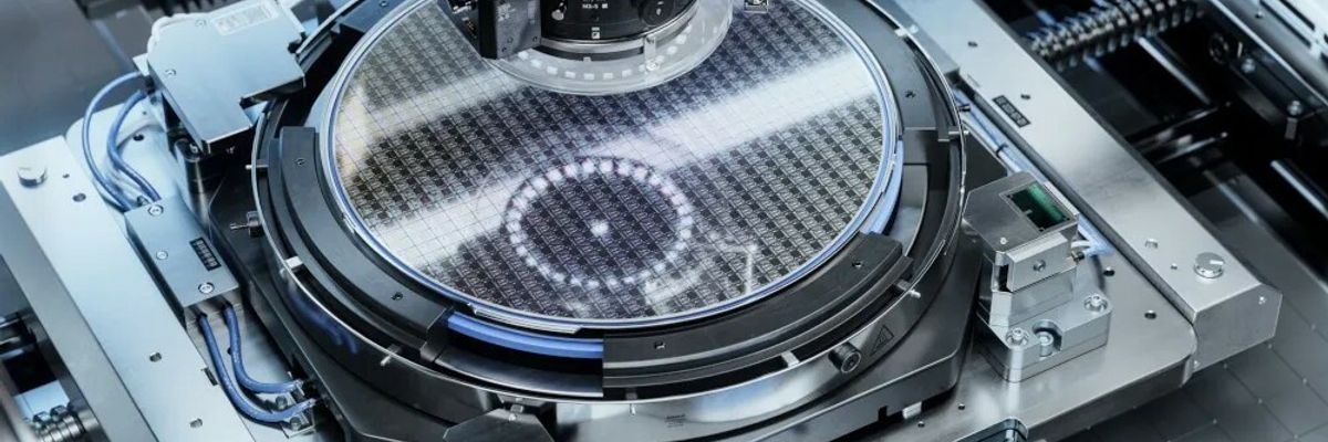
Accurate temperature control in optical lithography is critical to ensure consistent photoresist application, curing, and pattern transfer. Even minor temperature variations can lead to non-uniform layer thickness, defects in patterning, and reduced reliability of semiconductor devices. Additionally, lithography processes require temperature measurement directly on the wafer surface without physical contact, as any interference may compromise process integrity. Limited installation space and the need for high precision further complicate reliable temperature monitoring.
Solution
Infrared temperature measurement provides a non-contact and highly precise method for monitoring wafer surface temperature in real time. Long-wave spectral pyrometry enables accurate detection of temperature distribution directly on the wafer, even in confined semiconductor manufacturing environments. This ensures uniform photoresist coating, optimal curing conditions, and stable lithography performance.
Compact infrared sensors such as the CSmicro series are particularly well suited for these applications. Due to their extremely small sensor head and robust design, they can be easily integrated into tight spaces near the wafer. These sensors operate in the long-wave infrared range (8–14 µm), which is ideal for measuring temperatures on semiconductor surfaces with high accuracy. Their fast response time allows immediate detection of temperature changes, enabling dynamic process control and improved stability.
Benefits
Ensures uniform photoresist thickness, improving pattern precision and device performance
Reduces defects caused by temperature fluctuations, increasing yield and product quality
Enables precise, non-contact measurement without interfering with sensitive processes
Provides real-time temperature feedback for stable and optimized process control
Improves wafer processing uniformity, enhancing throughput and operational efficiency
The Crucial Role of Temperature in Semiconductor Optical Lithography
Optical lithography is a fundamental process in semiconductor manufacturing used to transfer circuit patterns onto a wafer. The process begins with coating the wafer with a photosensitive material known as photoresist. A photomask is then aligned over the wafer, and ultraviolet light is used to expose specific regions of the photoresist, initiating chemical changes.
Temperature plays a critical role in several stages of lithography. During photoresist coating and curing, precise temperature control is required to remove solvents and achieve a uniform layer thickness. Any temperature deviation at this stage can result in uneven coating, leading to pattern distortions in later steps.
After exposure, the wafer undergoes development, where the pattern becomes visible. Subsequent processes such as etching or deposition transfer this pattern into the substrate. Throughout all these steps, maintaining a stable and homogeneous temperature is essential to ensure accuracy, repeatability, and high-quality semiconductor structures.
Temperature Control in Lithography with Infrared Sensors
In lithography environments, direct contact temperature measurement is not feasible due to contamination risks and process sensitivity. Therefore, non-contact infrared sensors are essential for accurate monitoring.
Long-wave infrared sensors are particularly effective for this application, as they measure temperature directly on the wafer surface without being affected by reflections or environmental interference. Their ability to operate in tight installation spaces makes them ideal for integration into lithography equipment.
The CSmicro infrared sensors stand out due to their compact size, high precision, and reliability. Their miniature sensing head allows installation in confined areas, while maintaining accurate alignment with the wafer surface. The sensors support a wide temperature range from -40 °C to 1030 °C, making them suitable for multiple stages of semiconductor processing.
Additionally, their fast response time ensures immediate temperature feedback, which is critical for maintaining tight process tolerances. The sensors can be easily integrated into existing control systems via analog outputs, enabling seamless communication with PLCs and automated process control systems.
Enhancing Process Stability and Efficiency
Accurate temperature monitoring is essential for ensuring process stability in lithography. Infrared sensors provide continuous, real-time data that allows manufacturers to maintain consistent thermal conditions across the wafer.
This level of control reduces variability, minimizes defects, and improves overall production yield. By ensuring uniform temperature distribution, manufacturers can achieve higher precision in pattern transfer and better performance of semiconductor devices.
Modern infrared sensing solutions also contribute to improved efficiency. Faster response times enable rapid adjustments to process conditions, reducing downtime and increasing throughput. Reliable measurement systems reduce the need for rework and improve overall manufacturing productivity.
Temperature control is a critical factor in achieving high precision and reliability in optical lithography. Advanced infrared sensors provide a non-contact, accurate, and efficient solution for monitoring wafer temperature in real time.
Compact and high-performance devices such as the CSmicro infrared sensors enable precise measurement even in confined spaces, ensuring uniform processing conditions and improved semiconductor quality. By integrating these technologies into lithography systems, manufacturers can enhance process stability, reduce defects, and achieve higher production efficiency in modern semiconductor fabrication.


